Wafer Thermostat Wiring Diagram: The Simple HVAC Control Solution Globalfoundries and globalwafers partnering to expand semiconductor
If you are looking for From Crystals to Circuits: A Deep Dive into Wafer Processing - Atlanta you've visit to the right web. We have 25 Pictures about From Crystals to Circuits: A Deep Dive into Wafer Processing - Atlanta like What is a Wafer in VLSI – VLSIFacts, Time Series Classification Website and also GlobalWafers scores $400M for building 300mm wafer plants • The Register. Here you go:
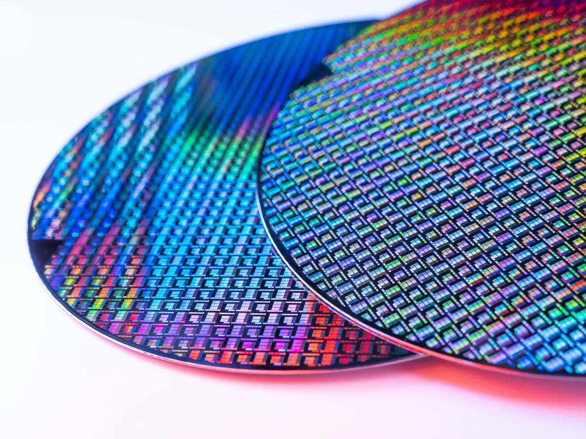
From Crystals To Circuits: A Deep Dive Into Wafer Processing - Atlanta
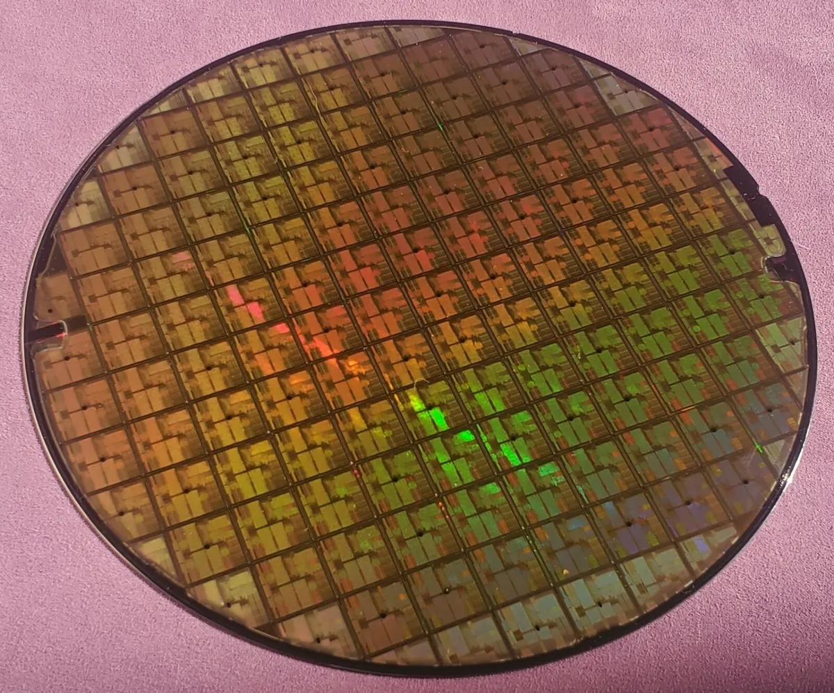 www.atlnightspots.com
From Crystals to Circuits: A Deep Dive into Wafer Processing - Atlanta ...
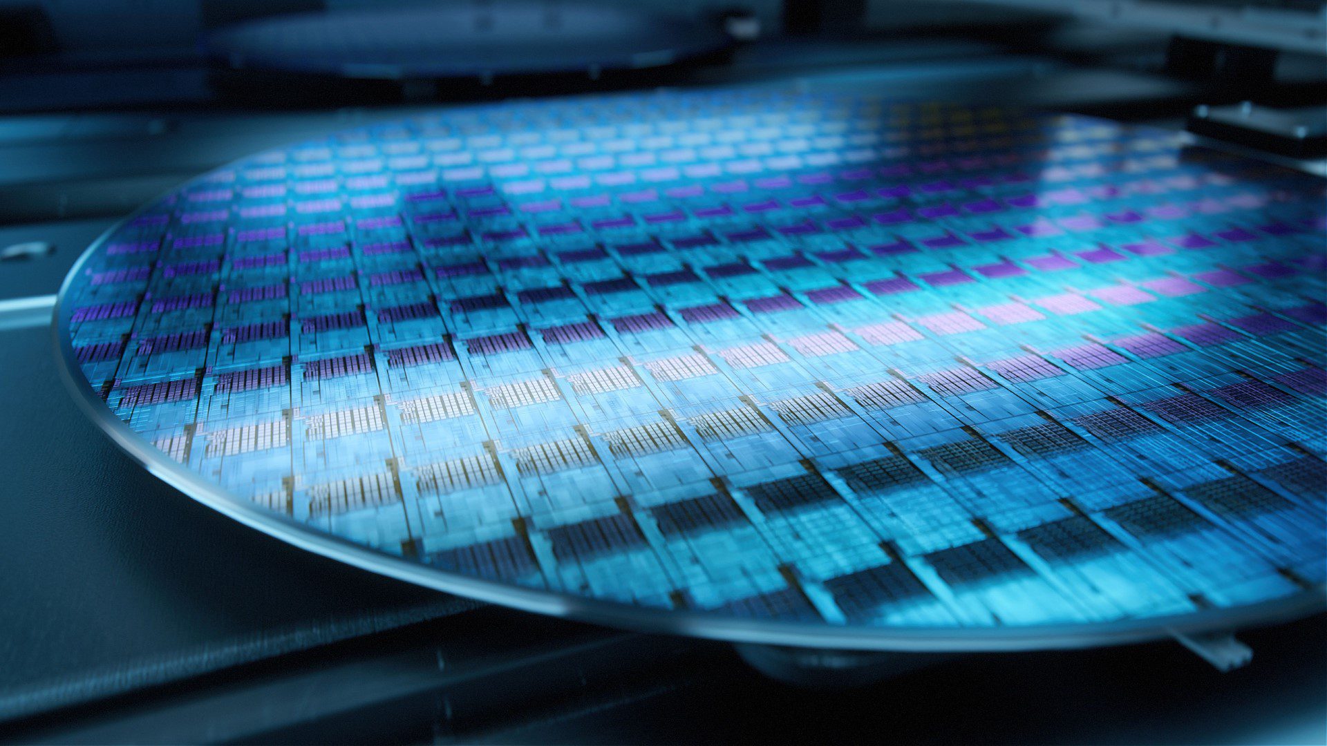
Wafer Silicon Manufacturing
 www.waferworld.com
wafer Silicon Manufacturing
TSMC Wil AMD En Nvidia Verleiden Met Prijsdalingen 3nm-wafers - ITdaily.
 itdaily.be
TSMC wil AMD en Nvidia verleiden met prijsdalingen 3nm-wafers - ITdaily.
Wafer - AnySilicon
 anysilicon.com
wafer - AnySilicon
What Is A Wafer? – WaferPro
 semiconductorwafers.wordpress.com
What is a Wafer? – WaferPro
What Is A Wafer Chuck?
 www.waferworld.com
What Is a Wafer Chuck?
Silicon Wafer Fabrication
 ar.inspiredpencil.com
Silicon Wafer Fabrication
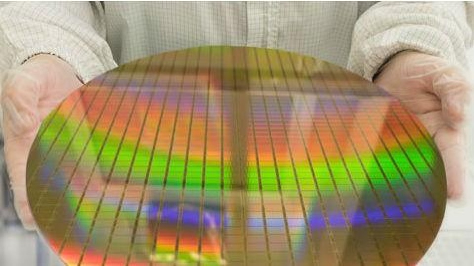
GlobalFoundries And GlobalWafers Partnering To Expand Semiconductor
 gf.com
GlobalFoundries and GlobalWafers Partnering to Expand Semiconductor ...
Europa Maakt Zich Sterk Voor 450 Mm Wafers
 www.agconnect.nl
Europa maakt zich sterk voor 450 mm wafers
WAFER Definition And Meaning | Collins English Dictionary
 www.collinsdictionary.com
WAFER definition and meaning | Collins English Dictionary
Silicon Wafer | Wafer Cleaning Process And Its Importance
 www.waferworld.com
Silicon Wafer | Wafer Cleaning Process and Its Importance
Edita Inaugurates A New Factory, Launches New Wafer Line. | Enterprise
 enterprise.press
Edita inaugurates a new factory, launches new wafer line. | Enterprise
Choosing The Right Wafer Material For Your Needs
-p-1080.jpg) www.waferworld.com
www.waferworld.com
Choosing the Right Wafer Material for Your Needs
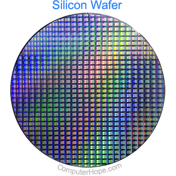
What Is A Wafer?
 www.computerhope.com
What is a Wafer?
What Is A Wafer In VLSI – VLSIFacts
 vlsifacts.com
What is a Wafer in VLSI – VLSIFacts
Wafer Semiconductor_LANScientific- For The Packet Lab
 en.lanscientific.com
Wafer Semiconductor_LANScientific- For The Packet Lab
Intel's Chip Manufacturing With 450mm Wafers Delayed To 2023 Due To Low
 wccftech.com
Intel's Chip Manufacturing with 450mm Wafers delayed to 2023 Due to Low ...
Wafer - 3 | An Interesting Wafer That I Picked Up. Read More… | Flickr
 www.flickr.com
wafer - 3 | An interesting wafer that I picked up. Read more… | Flickr
A Wafer Filled With Memristors [IMAGE] | EurekAlert! Science News Releases
A wafer filled with memristors [IMAGE] | EurekAlert! Science News Releases
Semiconductor Wafer | WaferPro
 www.waferpro.com
Semiconductor Wafer | WaferPro
GlobalWafers Scores $400M For Building 300mm Wafer Plants • The Register
 www.theregister.com
GlobalWafers scores $400M for building 300mm wafer plants • The Register
Time Series Classification Website
 timeseriesclassification.com
Time Series Classification Website
Ma Passion La Technologie: Qu’est-ce Qu’un Wafer
 h-techpassion.blogspot.com
Ma Passion la technologie: Qu’est-ce qu’un Wafer
Wafer Fabrication - NTP Semiconductor
 ntpsemi.com
Wafer Fabrication - NTP Semiconductor
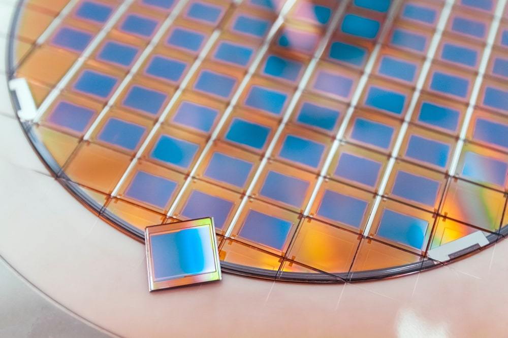
10 Surprising Uses Of Patterned Wafers: From Solar Cells To Wearable
 websta.me
10 Surprising Uses Of Patterned Wafers: From Solar Cells To Wearable ...
Wafer semiconductor_lanscientific- for the packet lab. Edita inaugurates a new factory, launches new wafer line.. Time series classification website